Paper on the Characterization of the Dielectric Properties of Commercially Available Low-loss UV-curable Resins from 60 GHz to 90 GHz
October 26, 2022 – At the recently held European Microwave Week conference in Milan, our colleague Paola Escobari successfully presented her work on the characterization of the dielectric properties of commercially available low-loss UV-curable resins from 60 GHz to 90 GHz.
Two dielectric properties
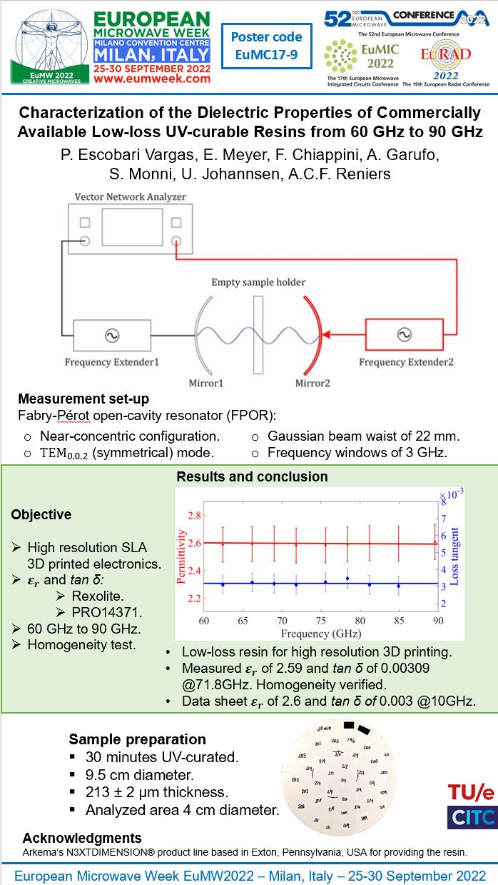 In her research, Paola determined two important dielectric properties, the relative permittivity and the loss tangent of a new commercially available UV-curable SLA resin sample. She performed the characterization of the dielectric material in the millimeter-wave range using an open-cavity Fabry-Perot resonator.
According to the manufacturer’s data sheet, the ultralow-loss photoresist material, optimized for advanced electronic applications, has a relative permittivity of 2.6 and a loss tangent of 0.003, both at 10 GHz.
First, Paola determined the accuracy of the Fabry-Perot open-cavity resonator using a reference material called Rexolite. Then, she measured the new dielectric material in a frequency band from 60 GHz to 90 GHz.
The results show that the new commercial resin sample has a relative permittivity of 2.59 and a loss tangent of 0.0031 at 71.8 GHz. This means that these materials for 3D printing are suitable for mmWave application and thus can be used in the development of e.g. antennas or packaging.
Interested in the complete results? Download paper
Innovation meets collaboration
Collaboration is vitally important in innovation. CITC has created an effective ecosystem in which companies, research and educational institutes work on bridging the gap between academics and industry.
Paola’s work is a perfect example of multi-party collaboration. She is an Engineering Doctorate student at Eindhoven University of Technology. Her work, however, is funded by and in collaboration with CITC.
In this particular project, she was supported by TNO Radar Technology department and TNO Holst Centre. The TNO branches not only manufactured the material samples used in this work, they also provided support and access to specialized equipment. In addition, the project was supported by Sartomer’s N3xtDimension product line and, finally, Antennex provided access to the Fabry-Perot resonator.
Photo credit to Elmine Meyer, Eindhoven University of Technology
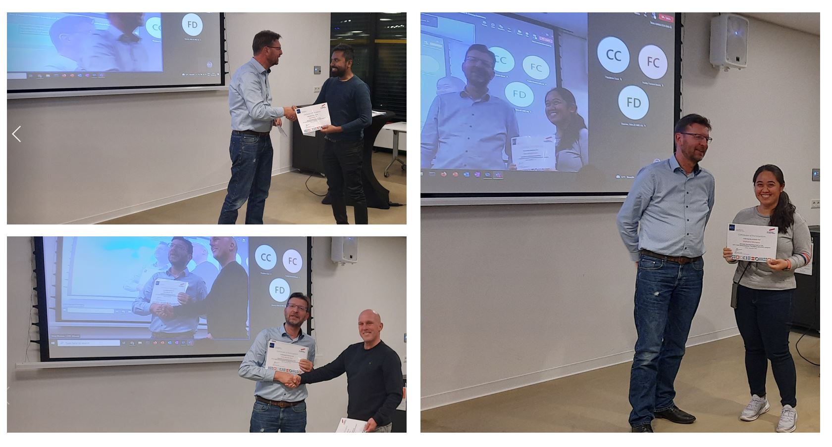
October 17, 2022 – On October 10, the industry participants of the Semiconductor Packaging University Program 2022 received their certificates. Some of them will continue with the practical part of the program, together with the bachelor student participants.
International students
The third edition of the program started on August 29 in hybrid form. Most students attended the live sessions that were held at the Noviotech Campus, but due to the geographical distance, some followed the program via a live stream. Education consultant Joop Bruines, also responsible for coordinating the program, comments: “This year, we had participants not only from Germany, but also from Brazil and the U.S. It is great to see that our program is being followed more and more internationally.”
Mix of bachelor students and semicon staff
Like the previous edition, this year’s program was offered as a minor to bachelor students and industry professionals. Bruines: “We have a nice mix of people. In addition to participants from companies such as NXP and Nexperia, there are eight bachelor students from HAN and similar Dutch universities of applied sciences and from Rhein-Whaal Hochschule in Cleves.” He is also pleased that seven of this year’s participants are female. “That is a first for us. As everyone knows there are too few women in high-tech. We hope that with our program we can contribute to an increase of women in the semicon industry in the future.”
Tailor-made program
CITC and HAN University of Applied Sciences (HAN), developed this program tailored to the specific needs of semiconductor companies. The program focuses on the design and manufacturing of semiconductor packages and the associated assembly, reliability and test techniques. It includes a practical assignment that will be carried out on the premises of either a semiconductor company or CITC.
On October 10, the last lectures of the theoretical part of the program were given. Afterwards, the industry participants who subscribed for this part only received a certificate for attending the course. The bachelor students and some of the industry participants will continue the next part of the program which consists of practical assignments.
Fourth edition
The next edition of the Semiconductor Packaging University Program is scheduled for August/September 2023. Interested in following the next edition of this program? Please contact us for more information or to receive the registration form.
August 29, 2022 – Today, the third edition of the Semiconductor Packaging University Program started at the Novio Tech Campus in Nijmegen. Twenty four participants attended the program live and four followed the live stream. Over the next five months, they will be introduced to the semiconductor industry and delve into the final step of chip manufacturing: chip packaging.
Tailor-made program
CITC and HAN University of Applied Sciences (HAN), developed this program tailored to the specific needs of semiconductor companies. The program focuses on the design and manufacturing of semiconductor packages and the associated assembly, reliability and test techniques. It includes a practical assignment that will be carried out on the premises of either a semiconductor company or CITC.
Mix of bachelor students and semicon staff
Like the previous edition, this year’s program will be offered as a minor to bachelor students and industry professionals. Joop Bruines, education consultant at CITC and also working at HAN, is happy with the full classroom: “We have a nice mix of people. In addition to industry participants from companies such as NXP and Nexperia, there are eight bachelor students from HAN and similar Dutch universities of applied sciences and from Rhein-Whaal Hochschule in Cleves.” He is also pleased that seven of this year’s participants are female. “That is a first for us. As everyone knows there are too few women in high-tech. We hope that with our program we can contribute to an increase of women in the semicon industry in the future.”
Hybrid format
The program has a hybrid format and as such offers the opportunity to participate when traveling to Nijmegen is not an option. Bruines: “Four students will be following the live stream, so we just went live in the U.S. and in Brazil!”
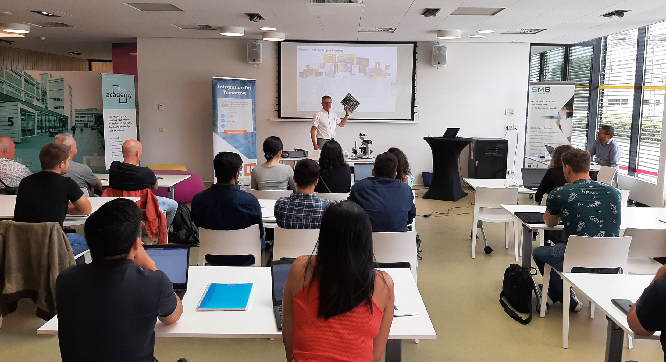
A printed circuit board serves as an aid at the start of Henk van Zeijl’s lecture
In his introductory speech, Bruines emphasized the importance of chips in everyday life and the need for well-trained people in this field. As a large part of the program takes place on the Novio Tech Campus, its director Bert Krikke gave a brief overview of the campus and the ambition to create an attractive ecosystem for companies in health and high-tech. After his presentation, Henk van Zeijl from TU Delft took over with the first lecture.
Interested in following the next edition of this program? Check out the program information or contact us.
August 22, 2022 – Last week, CITC welcomed a new addition to its lab: a high-resolution desktop Scanning Electron Microscope (SEM). The microscope combines an optical camera for never-lost navigation with detailed imaging and analysis. This should enable a completely new electron microscopy experience.
High-quality images
The high brightness offered by the SEM makes it easy to obtain high-quality images with many details. The SEM provides accurate and reproducible results that allow us to obtain the quality information we need to detect failures in samples early, and adjust our research process when needed. It is a good addition to our existing lab infrastructure.
Access to infrastructure
CITC’s lab facilities support the innovation programs and contribute to education through internships and MSc/PhD programs. Furthermore, our lab serves as demo and application lab for new types of equipment and materials. The lab is available to third parties to enable them to develop and implement new packaging solutions.
PRESS RELEASE | Nijmegen, the Netherlands and Irvine, CA | July 19, 2022
Chip Integration Technology Center (CITC) and Henkel announced today that the organizations have formalized an agreement to collaborate on the development of high-thermal die attach solutions for RF and power electronics. Under the terms of the partnership, Henkel will supply commercialized and developmental pressureless sintering die attach formulations and CITC will provide testing and analysis of the materials within next-generation package designs.
CITC’s Thermal High-Performance Packaging program focuses on thermo-mechanical design strategies and device packaging platforms that integrate low-stress, high-reliability rugged interconnect solutions. As die attach and molding materials are often limiting factors for the optimal operation of RF and power packages, Henkel is the ideal partner or innovation in this application area.
In addition to ongoing work in its state-of-the-art R&D centers, Henkel wants to accelerate time-to-market for its semiconductor packaging materials through strategic relationships across industry, government, and academia. CITC, which collaborates with leading power and RF device packaging companies, provides a unique opportunity to characterize and analyze Henkel’s high-thermal die attach formulations as an enabler for leading-edge device designs.
“Henkel’s pressureless sintering die attach materials are already proven in certain mobile applications,” explained Ramachandran “Ram” Trichur, the company’s Global Market Segment Head, Semiconductor Packaging Materials. “We want to extend that success to other sectors such as automotive, where large, high-power chips are the norm. Our pressureless sintering solutions are unique because they deliver the simple, low-stress processability of conventional die attach adhesives and very high thermal conductivity capabilities. The work at CITC will augment our in-house projects, allowing additional performance and reliability validation.”
The new die attach technology has the potential to enable the replacement of lead (Pb) within RF and power semiconductor devices that incorporate larger die on copper leadframes, allowing the introduction of high operating temperature gallium nitride (GaN) and silicon carbide (SiC) power die technologies. Many of CITC’s partners are actively integrating these new chip structures, making the cooperative project an excellent proving ground for Henkel’s pressureless sintering platform.
“In Henkel, we have found a material innovator that will enable the development of power and RF devices with a holistic approach that leverages the latest in die attach technology,” concluded CITC General Manager, Jeroen van den Brand. “With many major power device manufacturers based in Europe, and in Nijmegen in particular, we view this partnership as vital to satisfying the current and future demands within these important market sectors.”
– ENDS –
About CITC
Chip Integration Technology Center (CITC) is a non-profit joint innovation center specializing in heterogeneous integration and advanced chip packaging technology. CITC has created an effective ecosystem in which companies, research and educational institutes work on bridging the gap between academics and industry. CITC’s contribution to the ecosystem is to provide access to innovation, infrastructure and education.
www.citc.org
About Henkel
Henkel operates globally with a well-balanced and diversified portfolio. The company holds leading positions with its three business units in both industrial and consumer businesses thanks to strong brands, innovations and technologies. Henkel Adhesive Technologies is the global leader in the adhesives market – across all industry segments worldwide. In its Laundry & Home Care and Beauty Care businesses, Henkel holds leading positions in many markets and categories around the world. Founded in 1876, Henkel looks back on more than 140 years of success. In 2021, Henkel reported sales of more than 20 billion euros and adjusted operating profit of about 2.7 billion euros. Henkel employs about 53,000 people globally – a passionate and highly diverse team, united by a strong company culture, a common purpose to create sustainable value, and shared values. As a recognized leader in sustainability, Henkel holds top positions in many international indices and rankings. Henkel’s preferred shares are listed in the German stock index DAX.
www.henkel-adhesives.com/electronics
Contact
CITC: Marco Koelink | M +31 6 15 15 66 41 | E marco.koelink@citc.org
Henkel: Ruud de Wit | M +31 6 43 37 21 08 | E ruud.dewit@henkel.com
July 12, 2022 – We are deeply affected by the death of our colleague and figurehead of CITC: Barry Peet.
As co-founder, first employee and general manager, he was the driving force behind the informal, open culture in our organization and the many partnerships with companies, research institutions and knowledge institutes.
Barry obtained an MSc in Electronic Engineering from the University of Twente. With a background in both ICT and semiconductors, he started his first company in mobile solutions in 1999 during his studies. After 13 years leading this company, Barry became managing director of BCSEMI (currently: Holland Semiconductors). In this position, he helped strengthen and expand the Dutch semiconductor ecosystem. From 2017, Barry initiated and founded CITC and moved to the position of General Manager at CITC in 2019. As General Manager, Barry was responsible for the overall management of CITC.
CITC would not be what it is today without him. We will miss his energy, enthusiasm and enormous drive. Our thoughts and condolences go out to his family, relatives and friends. We wish them a lot of strength in this difficult period.
Employees, management and Supervisory Board CITC
April 21, 2022 – On April 25, CITC’s Henry Martin will present his work on in-situ reliability monitoring of power packages using a Thermal Test Chip at EuroSimE. The 23rd International Conference on thermal, mechanical and multi-physics simulation and experiments in microelectronics and microsystems is held in Malta.
Thermal test chip
Henry will discuss the crucial need to meet stringent automotive standards and to better understand the critical failure mechanisms of high-power electronics to improve their reliability. To that end, he* developed an in-situ reliability monitoring setup. This is capable of actively measuring the thermal performance of a package during lifetime testing.
A Thermal Test Chip (TTC – depicted above) assembled into a Power Quad Flat No-lead (PQFN) package was employed as a test vehicle for non-destructive reliability assessment. The TTC comprises resistive heaters as a heat source and resistive temperature elements for measuring the thermal response.
Transient thermal behavior
The team evaluated the transient thermal behavior based on the contribution of a heat source to a temperature field. They measured the temperature distribution at multiple spatial positions. The experimental results provide insights into the thermal properties’ influence on the thermal behavior of the package.
A compact electro-thermal model based on analogies was developed to deconvolute and analyze the transient thermal measurements. The results of the compact model correlate with the experimental measurements, and the model’s accuracy was verified using finite element simulations. The development of such thermal characterization experiments and computationally inexpensive models assist in further understanding the impact of failures in advancing high-power density electronics.
More information
If you’d like to know more about Henry’s work or the full publication, please contact him per email.
*in this project, Henry worked together with Romina Sattari[2], Edsger Smits[1], Henk van Zeijl[2], Willem van Driel[2,3] and Kouchi Zhang[2].
[1] Chip Integration Technology Center
[2] Electronic Components, Technology & Materials (ECTM) – TU Delft
[3] Signify Research
PRESS RELEASE | Nijmegen, the Netherlands, April 12, 2022
Chip Integration Technology Center (CITC) has signed a Memorandum of Understanding (MoU) with the Electronics & Photonics Innovation Centre (EPIC) in Torbay, UK. The move offers an exciting opportunity for both organizations to collaborate and benefit from the synergies that exist between the two centers.
EPIC is located within a rich cluster of microelectronics and photonics packaging specialists. The center offers businesses access to labs, offices, >€3M of prototyping capability and a classified cleanroom. Dutch-owned EFFECT Photonics have chosen EPIC as their R&D facility and have benefited from extensive local funding to support this growth. Other businesses located within EPIC include Spanish MEMS innovators Nanusens and photonics packaging specialists Bay Photonics.
CITC is a non-profit innovation center specializing in heterogeneous integration and advanced chip packaging technology for semiconductor and photonic applications. It is a place where companies, research and educational institutes work together on bridging the gap between academics and industry and creating a new generation of packages providing smart, safe and rugged housing for chips.
Share information
The MoU will see both parties sharing information with their respective businesses to showcase the technical capability and services on offer at both centers. EPIC and CITC will also be exploring opportunities to add each other’s centers to future funding bids with a view of generating additional revenue for both projects.
Both centers have close links to relevant universities and higher education partners therefore encouraging collaboration between academia will also be explored.
Many opportunities for collaboration
EPIC Centre Director, Wayne Loschi, is excited about the partnership: “There are so many clear opportunities for collaboration which will benefit our respective centers and our businesses. We’d love to see our companies working closer with CITC to improve innovation and equally we’d welcome more Dutch companies to join EFFECT Photonics within EPIC”.
CITC Business Development Manager, Marco Koelink, is also looking forward to starting the relationship: “EPIC offers a rich ecosystem in microelectronic and photonic R&D and assembly activities. Collaboration, especially in photonic packaging is crucial to develop high-volume and low-cost solutions for meaningful application areas such as communications, medical and automotive. CITC and EPIC jointly strengthen their value proposition in providing access to innovation, infrastructure and education”.
Contact
To find out more about CITC, its technology, programmes, activities and the services it offers please contact: Marco Koelink
To find out more about EPIC, accessing its technicial capability, regional funding up to £150k and support obtaining UK R&D tax credits please contact: Wayne Loschi
April 5, 2022 – With spring 2022 approaching, it is time to look back at 2021. A year that was dominated by COVID-19. However, this did not stop us from providing access to innovation, infrastructure and education. We have summarized our results in the infographic below.
Highlights
While many people were still working from home, CITC expanded its lab facilities. The new equipment allowed our colleagues in the lab to continue working steadily on optical alignments and chip placement, while using lots of wire to make wirebonds.
In August, we launched the second edition of the Semiconductor Packaging University Program. Nineteen participants, both students from various universities of applied sciences and semiconductor employees, followed the program and took a deep dive in the world of semiconductor packaging.
Finally, live events were possible in autumn. First, we attended PIC International in Brussels. Next, we went to Germany and presented ourselves at SEMICON Europe in Munich. It was a revelation to meet people in person after all those Teams and Zoom meetings in previous months. With many new contacts, there were plenty of exciting projects to work on.
New possibilities
All in all, we are proud of what we achieved last year. Now that the COVID-19 measures have been lifted in the Netherlands and the rest of the world is also opening again, there are so many opportunities to meet our customers and students.
We have already received several students groups in our labs and more will follow. We plan to attend many live events, exhibitions and conferences. The first large event on our agenda is PCIM Europe. Please check out our event calendar for all other events. We are eager to meet you!
And, of course, registration for the third edition of our Semiconductor Packaging University Program has begun. We look forward to training yet another group of students in semiconductor packaging.
So stay tuned for what’s to come!
Downloads
March 31, 2022 – Special visitors for CITC on an ordinary Sunday morning in March: more than 30 students from Weekendschool Nijmegen came by for a lesson in chip packaging. The guest lecture is part of the Weekendschool’s ‘New technology’ theme for its first-year students. The CITC team was happy to oblige.
Many questions
The lecture started with a presentation about chip packaging. CITC’s business development manager Marco Koelink incorporated several short video clips in his story. The students (aged 10-11 years) were given the opportunity to ask questions and made full use of it. Like their fellow students in Arnhem, they were intrigued by the fact that the equipment that makes chips also contains chips. The materials used in chip packaging also raised eyebrows: “Is all that real gold on those chips?”
Marco noticed that most of the questions came from the girls. He is pleased with that. “It’s very important for girls to consider a choice for technology because there are simply too few women working in this industry”.
Lab tour
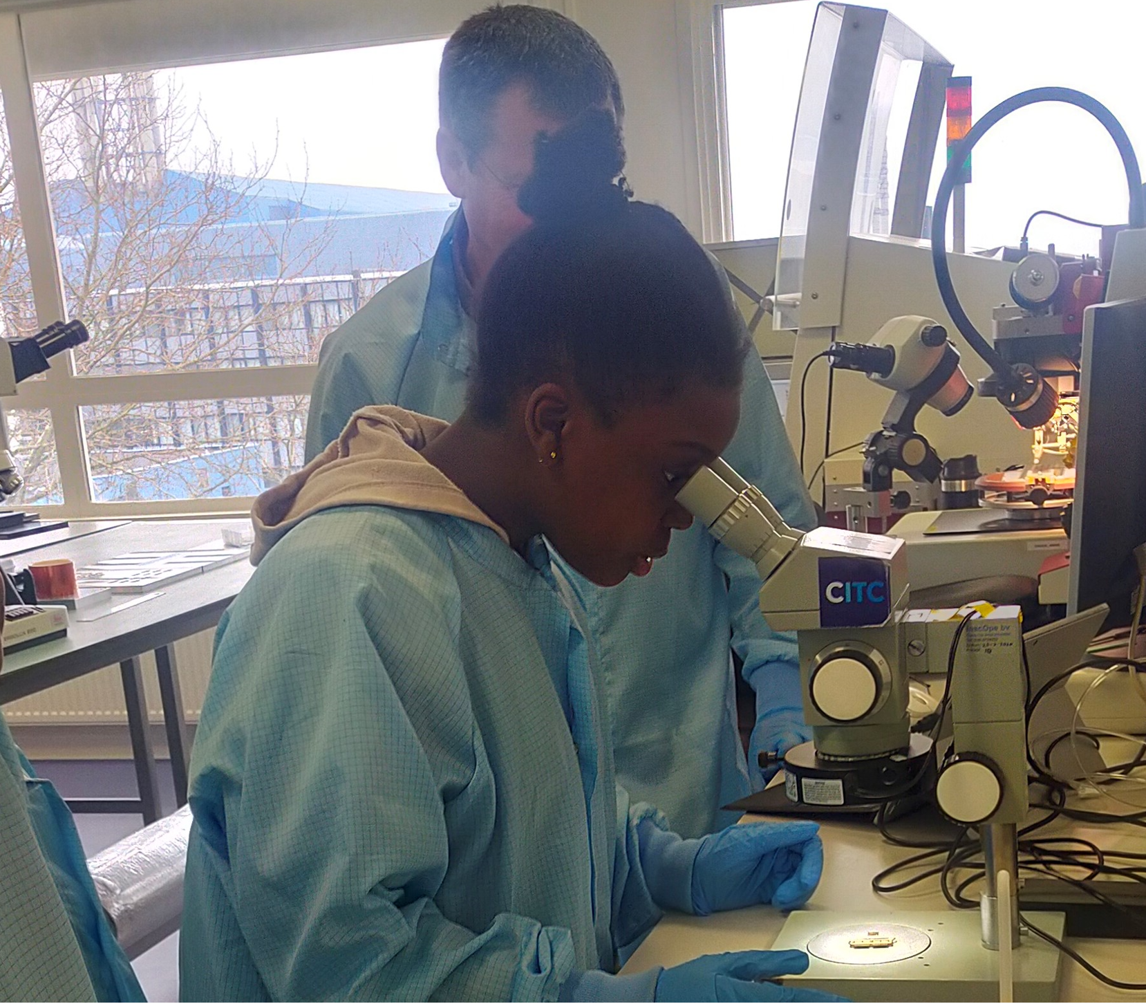
The next part of the program was a lab tour. Before entering the CITC labs, all students were required to dress up in lab coats and gloves. This resulted in a lot of giggles and selfies. Once in the labs, they were able to take a detailed look at equipment such as a die bonder and various microscopes. The students enthusiastically participated: “In the laboratory we were allowed to touch everything. And we could see through a really good microscope. That was cool!”
Practical assignment
The last part of the visit consisted of a practical assignment. The students were to build so-called ‘vibrating robot animals’ (in Dutch: bibberbeestjes). Using tools as screw drivers and cutting pliers, this turned out to be not an easy, but also a very fun task. Again, this lead to a lot of giggles once the batteries were in place and the robot animals vibrated on the tables.
Weekendschool Nijmegen location manager Chris van Wieren noticed how eager his students were. “Looking through a microscope, a machine that does what you say on command, a huge elevator in which machines are transported… you could see the wonder in the students’ eyes during our visit. They are already curious about the world of technology. To further enthuse them, all you need are professionals who can talk passionately about their daily work. Now, thanks to CITC, our students have become a bit more knowledgeable.”
Access to education
Providing access to education is one of CITC’s core activities. By enthusing children at an early age for technology in general, and perhaps a technical education and profession more specifically, we want to contribute to the future of the semiconductor industry in Europe.
Please feel free to contact us if your school is also interested in a CITC guest lecture or company visit.