CITC presents joint project results at ECTC
June 1, 2023 – CITC’s PhD candidate Henry Martin participated in the 73rd iEEE Electronic Components and Technology Conference (ECTC) in Orlando, Florida. He presented his paper titled ‘Heterogeneous integration of diamond heat spreaders for power electronics application’. The paper describes the results of a joint collaboration between CITC, Delft University of Technology and Mintres.
ECTC is an international event that brings together the best in packaging, components and microelectronic systems science, technology, and education. The technical program contains papers covering leading edge developments and technical innovations across the packaging spectrum.
Incorporating diamond heat spreaders in packages
 Within its Thermal High-Performance program, CITC often collaborates with both academic and industry parties. In this case, the research partners were Delft University of Technology and Mintres. Mintres manufactures chemical vapor deposition (CVD) diamond. This is a leading thermal management material with thermal conductivity up to 1800 W/mK. That is five times the thermal conductivity of pure copper.
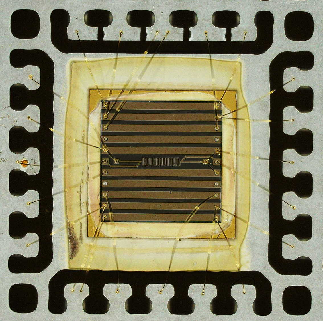
In this particular project, CITC has demonstrated that incorporating diamond heat spreaders in surface mount packages, such as a Power Quad Flat No-Lead (PQFN) packages, provides an efficient heat spreading solution.
Project highlights
At the conference, Henry presented some highlights of the research project:
- Optimizing the semiconductor substrate thickness and incorporating a diamond heat spreader resulted in approximately a 10% reduction in junction temperature compared to a standard package with a non-optimized semiconductor substrate and no heat spreader.
- Addition of a diamond heat spreader reduces the thermal gradient on the active surface of the device.
- The efficiency of the diamond heat spreader scales with the amount of input power applied to the active device.
 The conclusion of the paper is that heat sinks alone are not sufficient for concentrated micro-thermal hot spots. Therefore, heat spreaders are the go-to solution with increasing thermal challenges in high-power semiconductor devices.
The paper will soon be available in the iEEE xplore conference proceedings.
May 8, 2023 – CITC is pleased to present its annual results infographic. Looking back at 2022, this was the year in which we were finally able to expand our boundaries. Whereas in previous years, the focus was necessarily on the Netherlands, we now turned our attention to other countries, particularly Europe and Japan.
Highlights
Physical visits to customers and partners across the border, but also participation in international conferences and exhibitions – it was all possible again and we made ample use of that. This resulted in many new contacts, relationships, and partnerships.
We succeeded in creating a complete ecosystem for each of our three program lines. For each program, we built relationships with material suppliers, equipment suppliers, and internal device manufacturers. As a result, we now bring together knowledge and experience from different angles to create an optimal balance between design, material, and process.
The third edition of our Semiconductor Packaging University Program had more participants than ever before: 27 people attended the program.
And we expanded our lab infrastructure to keep supporting the innovation programs and contributing to education through internships and MSc/PhD programs.
Ready for growth
All in all, we are proud of what we achieved last year. We have experienced how applicable the adage ‘Think globally, act locally’ is to us. By working together locally, we can make a global impact: developing crucial solutions for the societal challenges that await us now and in the future.
For 2023, our main ambition is to grow. Grow in all kinds of areas: in the number of colleagues, in (lab) space, but especially in challenging innovative projects and in the number of students that we train* and coach. So stay tuned for what’s to come!
Downloads
CITC 2022 results infographic (EN)
CITC 2022 results infographic (NL)
* Registration for the fourth edition of our Semiconductor Packaging University Program has already begun
BLOG | May 2, 2023 – We all know that role models are important in everyday life. What girl wouldn’t want to have Serena’s tennis skills, sing like Beyonce or, more simply, buy her own flowers like Miley? This world doesn’t just need more Serenas, Beyonces or Mileys. What we desperately need is more women in science. But where are the role models there?
CITC, being an innovation center in chip packaging, is largely populated by men. There is one exception though. The team focused on RF chip packaging consists of five women and only one man. Program manager is Francesca Chiappini. She has a PhD in physics and has been working in science ever since. When we talk about her school and professional career, one thing stands out: she was always surrounded by female role models.
Role models everywhere
Francesca was born and raised in Genoa, Italy. All the women in her family had jobs outside the home. Her grandmothers were both entrepreneurs and her mother and aunt were both academically trained. “My mother studied physics and worked as a secondary school teacher. Her friends and colleagues who regularly came for dinner, all had a technical background”. At her own secondary school, Francesca’s teachers for the technical subjects were all women as well.
With such a background, it seemed obvious that Francesca would opt for a technical further education. However, it took a mini-internship with the biophysics group in the physics department of the University of Genoa to change her study plans from biology to physics. “As a child, I was not a nerd. Not the kind of person who takes things apart and tries to put them back together. I did love space travel and especially the stories behind it. In the mini-internship I got the chance to work with cells from rat brains and it finally made sense: it was going to be physics after all”.
She studied at the University of Genoa and came to the Netherlands in the Erasmus exchange program. As she loved the curriculum on solid state physics, she returned to Radboud University in Nijmegen after graduating to do her PhD on this subject.
Make a difference to the world
After obtaining her PhD, Francesca started working at TNO. Her traineeship consisted of two periods at TNO Delft and then at Holst Centre in Eindhoven. She stayed there after her traineeship ended. In 2019, Holst Centre seconded her to the then newly started Chip Integration Technology Center (CITC). In her role as program manager of the RF Chip Packaging program, Francesca could put together her team. “It is by sheer coincidence that the team is now largely made up of women. In the application procedures, the ladies turned out to be the best candidates. And once they joined the team, they didn’t want to leave”.
Being a program manager means attending a lot of meetings, not only at CITC and Holst Centre, but also with customers and within international projects. “Usually, I am the only woman present. And sometimes, I experience some bias being a woman and young”. Yet, Francesca loves her job. “I have a great job: I do what I want, what I like, and find it challenging. I do cool things, I learn new things, and contrary to popular belief: science is not boring at all. Physics is inspiring and as few people study it, it is special. It is a field that offers many opportunities, especially for women. You can combine your creativity and intelligence to make a difference to the world”.
Working with nerds
What about the prejudice that people who like physics are nerds? “Working with nerds is fantastic! It is all about science. There is no pressure to act a certain way, dress or adopt a lifestyle. You are judged less on things outside of work. That is a relief; you can be who you are. And by the way: you don’t have be a nerd to be good at science”.
Becoming a role model herself, Francesca has one last tip for aspiring female scientists: “Always introduce yourself with your name, title, and the fact that you have certain responsibilities. It may sound petty, but I’ve found it really works to dispel unconscious biases”.
In the picture from left to right: dr. Victoria Gomez-Guillamon Buendia – antenna designer, dr. Francesca Chiappini – program manager and dr. Tindara Verduci – cleanroom research scientist
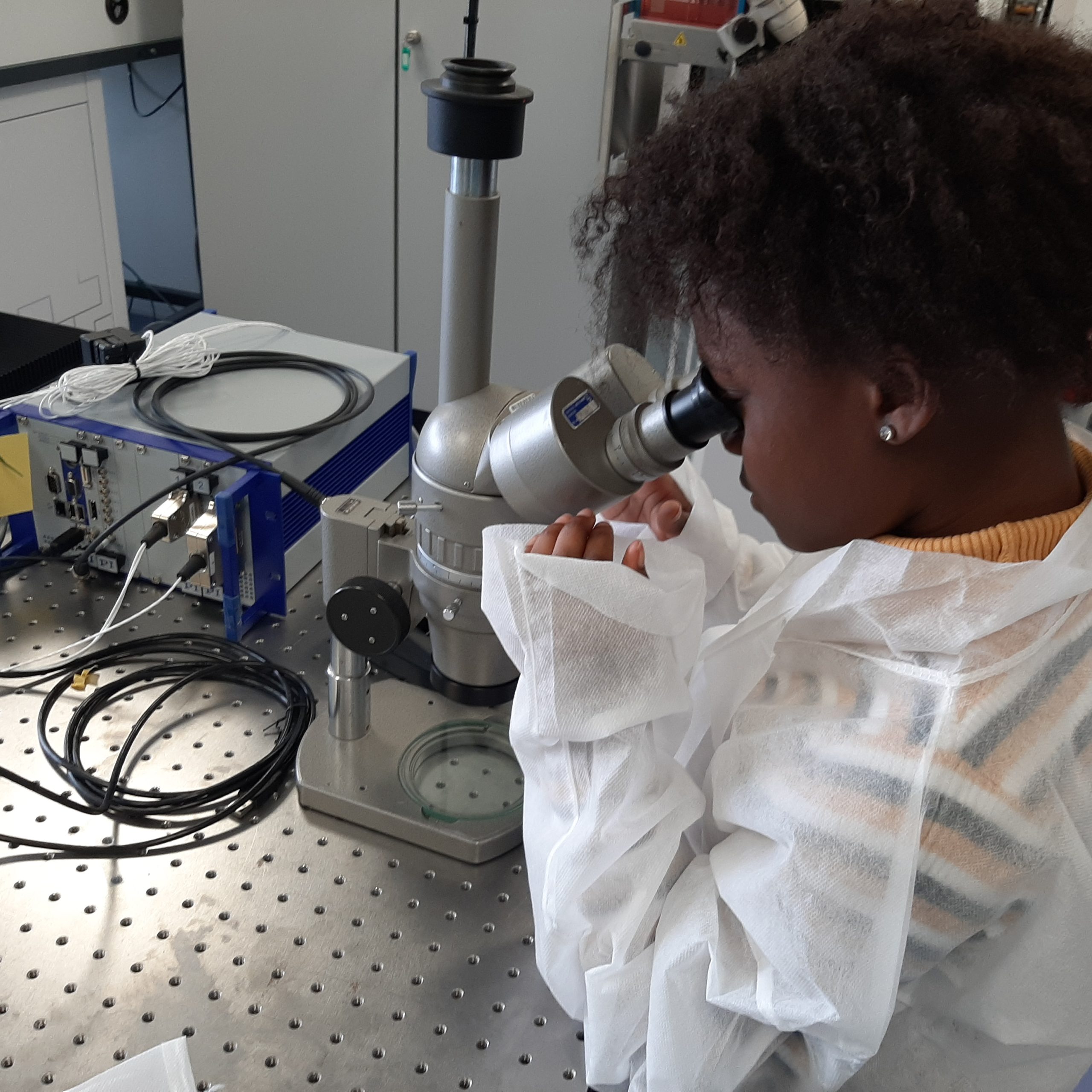
March 31, 2023 – On Sunday March 26, CITC received very special visitors on their site: 28 students from Weekendschool Nijmegen. For the second consecutive year, we provided a guest lecture within the theme ‘New Technology’ for the Weekendschool first-year students.
Many questions
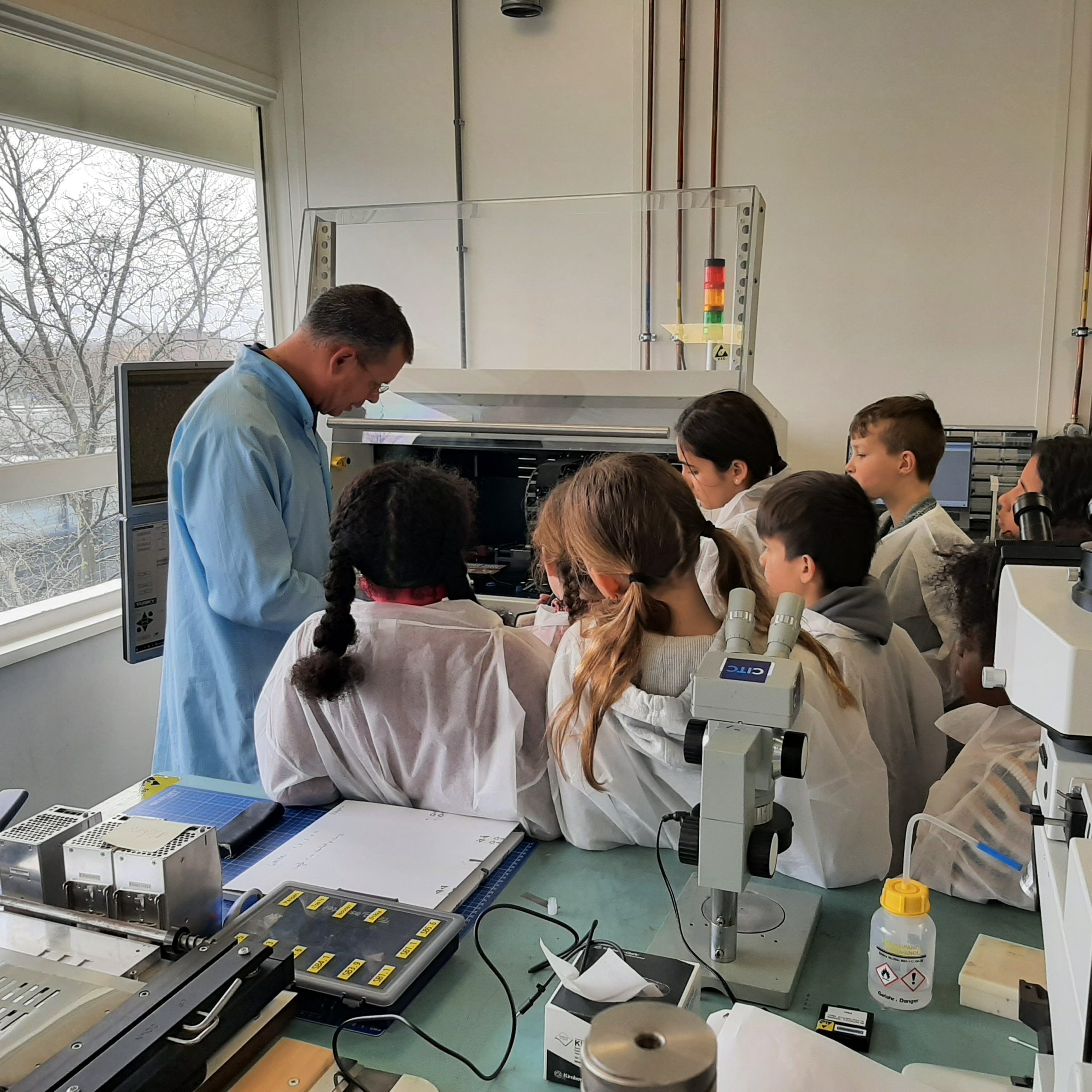
The program consisted of a mix of a lecture on chip packaging, a tour of the laboratories and working on a practical assignment: making so called vibrating robot animals – in Dutch: bibberbeestjes. During the lecture, CITC’s business development manager Marco Koelink hardly had enough time to answer all the questions. Some of the students (aged 10-11 years) wanted to know all ins and outs, it was obvious that they already had a previous lecture about chips at NXP.
Touring the labs
The tour of the laboratories always starts with a changeover moment: the students were required to dress up in lab coats. After that, they were all set to see in real life all the equipment they just learned about in the lecture. Lab manager Martien Kengen had prepared several samples to show them the processes of die placing and wire bonding. As always, the microscope was a big hit. The students were amazed at the level of detail they could see from the tiny chip. Weekendschool Nijmegen location manager Sarah van Dronkelaar noticed how eager her students were: “I heard one of my students say: I actually wanted to study architecture, but I like chips much more!”
Perseverance
 The students also worked on a practical assignment and with the help of tools as screw drivers and cutting pliers, they managed to create a nice variety of bibberbeestjes. When all groups had their bibberbeestjes ready, it was time for an actual race. This resulted in spinning robot animals, excited children, and a lot of laughter. Unfortunately, not a single bibberbeestje managed to reach the finish line. In his closing remarks, CITC’s program manager education Nathan van den Dool drew a nice parallel with science in practice: “In research, not everything succeeds the first time. You have to persevere. Very often, you have to further refine or adjust a design so that it eventually does what you want it to do.”
Access to education
Providing access to education is one of CITC’s core activities. By enthusing children at a young age about technology in general, and perhaps a technical education and profession in particular, we want to contribute to the future of the semiconductor industry in Europe.
Please feel free to Nathan van den Dool if your school is also interested in a CITC guest lecture or company visit.
March 23, 2023 – On March 1, CITC said goodbye to two interns who had been with us for just over a year: Ted Guijt and Nils Sistermans. The two ROC Nijmegen students in Creative Technology were working on a new demo: an enlarged chip package including a video screen for trade shows.
Chip packaging demo
In February last year, Ted and Nils started at CITC when one of their teachers asked them to follow up on a project started by a fellow student. For both students it was their first internship: two days per week. Nils had no expectations beforehand, but Ted was pleasantly surprised. “I had expected a very strict work environment compared to school, but that was not the case. Everyone was very open and friendly. We often made jokes with each other”.
The assignment they had to continue consisted of designing a demo that would stand out on trade shows. The students came up with a neat design of a chip package including LED lights aiming at a video screen in the middle. After approval of the design, they started to realize it. Nils: “At first glance, the assignment seemed quite simple. Later, however, we ran into many practical problems that we had to consider. For example, when a board cracked, the delivery time for a new board was longer than we expected”.
Pleasant working environment
As the demo is not completely finished yet, two new students will take over in due course. That was a bit of a disappointment but both students liked the internship itself. Nils: “CITC offers a very pleasant working environment, and I felt I could learn something from everyone”. Ted adds: “I really enjoyed the internship. The environment is stimulating, and I also liked the Noviotech Campus. And the colleagues were very helpful”. Both students agree that the internship fitted well within their education. “Many things we had learned at school, we could now apply in practice”, says Nils.
They both now move on to another internship. When asked to characterize their CITC internship in three words, Ted chooses fun, educational and openness. He has also recommended CITC to fellow students: “I told them about my positive experience, the good supervision and the fact that the internship is generally fun”. Nils opts for high-tech, challenging and also fun. “I would definitely recommend this internship to other students. However, I think that it is not suitable for everyone. This kind of internship requires a lot of independence and a good basic knowledge of electronics and mechanics”.
Wanted: new students
Interested in an internship or graduation assignment at CITC? Check out the opportunities or send an open application.
February 13, 2023 – On February 3, CITC student Marco De Martini successfully defended his graduation project at Fontys University of Applied Sciences in Eindhoven. He now has a bachelor’s degree in electrical and electronics engineering.
State-of-the-art equipment
When Marco started his assignment in September, he barely knew anything about semiconductors. “I wanted to learn more about semiconductors. They fascinate me as they are essential components of modern everyday life”, he explains. During his internship, Marco worked on the electro-thermal characterization of wideband gap devices. “In my assignment I got to work with the state-of-the-art equipment in the CITC lab. Most of the equipment, such as the in-situ climate chamber, was new to me so I was excited to learn how to work with it.”
Knowledgeable colleagues
Since CITC is not a very large organization, it is probably not the most obvious choice if you want to learn more about semiconductors. However, Marco’s choice for CITC, was prompted by the fact that the organization is small. “I like that you are not a number and that you have many opportunities to learn a lot. The colleagues are very knowledgeable and willing to help. I got to do a trial presentation and received useful feedback and support. This helped me to prepare for the final presentation”.
Asked to describe his internship in three words, he opts for family, inquisitiveness and high-tech. “The CITC team is small, which makes it more dynamic to talk to everyone. The colleagues were open and very welcoming. What I also liked is that everyone is open to each other’s work. Over lunch, we had broad conversations, both work-related and beyond. So, I can definitely recommend CITC to other students.”
Plans for the future
Now that he has completed his bachelor’s degree, Marco is ready for the future. Despite his American/Italian origins, he intends to stay in the Netherlands. “The Netherlands offers so many opportunities for engineers”, he explains. “I will first gain work experience. Ultimately, I would like to start my own business in solar panels. I have a background as an architectural draftsman, so I plan to combine this with my current education to work on smart homes”.
Wanted: new students
Interested in an internship or graduation assignment at CITC? Check out the opportunities or fill in our internship application form.
In the picture above, Marco is standing in front of the climate chamber, the CITC in-situ test set-up, which was a big part of his project.
January 26, 2023 – On January 25, the seven students who followed the CITC/HAN Semiconductor Packaging minor all passed their final exams. They presented the results of the practical assignments they worked on in the CITC laboratories and successfully defended their work.
Open laboratories
Although the students attended the third edition of the minor, they were the first to fully benefit from the program. The previous editions were overshadowed by the COVID-19 pandemic. This meant that the students at the time were unable to work on practical assignments. Now the CITC laboratories were open and the students could work with the equipment.
Ruben Pranger, Junior Technician at CITC – far right in the picture above, was responsible for supervising the practical work. He noticed that not all activities were equally popular: “The students weren’t too keen on measuring. However, when we moved to die shearing, they were really interested. ‘Dies can fly!’ was what they discovered while testing the attachment of the die to the leadframe.”
Hard work and fun
Joop Bruines, Education Consultant at CITC and program coordinator of the minor, recognizes the pleasure the students experience while working hard. He also enjoyed working with the group from September to now: “This year the group was very diverse in every way. We had six nationalities and the students came from four different universities of applied sciences, two of which were from outside the Netherlands. Their background also varied from the obvious mechanical engineering and electrical engineering to the less obvious chemical engineering and energy and materials science. Fortunately, there was a common ground that they all wanted to learn and have fun. I heard one of them say that he had never learned so much in such a short time”.
After the practical work, the students presented their findings and reports to Ruben and Joop as well as to HAN examiner Jeroen van Elburg (far left in picture above). They all passed the final test and received a certificate. CITC congratulates all students and wished them all the best in their future careers!
Next edition
For those who are interested in the next edition of the minor or the Semiconductor Packaging University Program for professionals, please read on here or contact us for more information. The program starts on August 28.
PRESS RELEASE | Nijmegen, the Netherlands | January 19, 2023
Chip Integration Technology Center (CITC) will intensify its cooperation with acoustic microscopy expert PVA TePla Analytical Systems GmbH. The cooperation offers exciting opportunities for both organizations to benefit from the synergies that exist between them.
Successfully determining which materials and processes are reliable for packaging is crucial to the mass commercialization of power and WBG semiconductors. Flawless basic materials are the key to flawless products. Cracks, cavities, detachment, or inclusions result in failures during the subsequent production process, which can be avoided with the help of reliable material analysis.
To realize this in its Thermal High-Performance packaging program, CITC is going to use the PVA TePla Scanning Acoustic Microscopy (SAM) 302 HD2 system. The microscope system provides non-destructive quality control capabilities and will therefore allow CITC to assess the reliability of the sinter die attachment to the leadframe.
The collaboration will also see both parties sharing information with their respective businesses to showcase the technical capability and infrastructure on offer at both organizations. Finally, PVA TePla and CITC will be exploring opportunities to jointly develop research opportunities.
Peter Czurratis, Managing Director of PVA TePla is excited about the partnership: “CITC is an upcoming and leading research center focused on new semiconductor wafer technologies and new trends in packaging and systems integration. Their cooperation with semiconductor companies and universities provides us with an excellent research platform for defining our future roadmap for the next generation of acoustic microscopes.”
CITC Business Development Manager, Marco Koelink, is also looking forward to this collaboration: “PVA TePla is one of the leading suppliers of Scanning Acoustic Microscopes. Through this collaboration, CITC will gain access to advanced analytical capabilities that will help us not only to analyze and identify bond layer failures, but also better understand material performance and predict failures at an early stage. That is a crucial capability in the development of robust and reliable bonding technologies.”
– ENDS –
About CITC
Chip Integration Technology Center (CITC) is a non-profit joint innovation center specializing in heterogeneous integration and advanced chip packaging technology. CITC has created an effective ecosystem in which companies, research and educational institutes work on bridging the gap between academics and industry. CITC’s contribution to the ecosystem is to provide access to innovation, infrastructure and education. CITC was founded in 2019 with strategic partners TNO and Delft University of Technology and powered by Holland Semiconductors. It is also supported by local and regional governments.
www.citc.org
About PVA TePla
With experience and know-how, PVA TePla AG has for many years supported important manufacturing processes and technological developments, primarily in the semiconductor, hard metal, electrical/electronics, and optical industries, but also in the forward-looking fields of energy, photovoltaics, and environmental technology.
https://www.pvatepla.com/en
***
Contact
CITC: Marco Koelink | M +31 6 15 15 66 41 | E marco.koelink@citc.org
PVA TePla: Peter Czurratis | M + 49 17 15 65 88 56 | E peter.czurratis@pvatepla.com
PRESS RELEASE | Nijmegen, the Netherlands | January 16, 2023
Chip Integration Technology Center (CITC) today announced the appointment of Mark Luke Farrugia as its new general manager. As of March 1, Farrugia will take over the responsibilities from general manager Jeroen van den Brand, who fulfilled the role ad interim.
Farrugia has an extensive background in the semiconductor backend industry. Prior to this appointment, he worked for almost sixteen years at NXP Semiconductors and most recently as technical director at Nexperia Semiconductors.
He explains why he is now switching to CITC: “Innovation work within semiconductor packaging has been my greatest professional passion for the past 27 years. Breakthrough innovation requires a dedicated organization having the right focus, knowledge and passion and determination, and I see this in CITC”.
In his position as general manager, Farrugia will be responsible for the further development of CITC as an internationally distinctive and well-recognized center of semiconductor and photonic chip packaging technology. “CITC is a young organization, and therefore needs to put itself on the semiconductor packaging map. This should be done by understanding the needs and expectations of the industry, building and enhancing the right competences, and by collaborating with other organizations. I look forward to working with the CITC team, as well as scouting and mentoring the next generation, dealing with the highly complex puzzle of understanding what the various industry stakeholders would like to achieve, and ultimately, to delivering results that have a meaningful impact on the industry.”
Roel Fonville, chair of the CITC Supervisory Board, expresses that this is what qualified Farrugia for the position at CITC: “The Supervisory Board is enthusiastic about the appointment of Mark Luke Farrugia as general manager of CITC. Mark Luke has substantive expertise, an up-to-date business network, entrepreneurial thinking and a strong drive to further internationalize CITC as an innovation center in the field of packaging.”
The position of general manager became vacant following the sad passing of CITC founder and first general manager Barry Peet in July 2022.
– ENDS –
About CITC
Chip Integration Technology Center (CITC) is a non-profit joint innovation center specializing in heterogeneous integration and advanced chip packaging technology. CITC has created an effective ecosystem in which companies, research and educational institutes work on bridging the gap between academics and industry. CITC’s contribution to the ecosystem is to provide access to innovation, infrastructure and education. CITC was founded in 2019 with strategic partners TNO and Delft University of Technology and powered by Holland Semiconductors. It is also supported by local and regional governments.
www.citc.org
Contact
Christian Ketelaars, Marketing & Communications Officer
E christian.ketelaars@citc.org
M +31 (0)6 48 15 42 92
November 25, 2022 – On November 23, delegates of the Provincial States of Gelderland visited CITC and the Noviotech Campus. As one of the subsidy providers, the province of Gelderland has been actively involved in CITC since 2019. We were proud to present what we have accomplished with their investment over the past 3.5 years.
CITC journey
First speaker of the day was Bert Krikke, managing director of Noviotech Campus. He informed the guests about the ambitious plans of the campus. Jeroen van den Brand, CITC’s general manager, was next. In his presentation he took the delegates through the ‘CITC journey’: what we have done so far, where we are now and what the future plans and ambitions are. To complement his story, Joep Stokkermans, innovation manager at Nexperia, and as such a customer of CITC, shared his experiences.
Lab tour
Final part of the visit was a quick tour through the CITC labs. Here, the delegates could see how we provide access to innovation, infrastructure and education in real life. Next to the state-of-the-art equipment, they saw bachelor students of the Semiconductor Packaging minor at work.
Photos by Sami Al Saiadi – Province of Gelderland