Looking back on 2021: CITC results infographic
April 5, 2022 – With spring 2022 approaching, it is time to look back at 2021. A year that was dominated by COVID-19. However, this did not stop us from providing access to innovation, infrastructure and education. We have summarized our results in the infographic below.
Highlights
While many people were still working from home, CITC expanded its lab facilities. The new equipment allowed our colleagues in the lab to continue working steadily on optical alignments and chip placement, while using lots of wire to make wirebonds.
In August, we launched the second edition of the Semiconductor Packaging University Program. Nineteen participants, both students from various universities of applied sciences and semiconductor employees, followed the program and took a deep dive in the world of semiconductor packaging.
Finally, live events were possible in autumn. First, we attended PIC International in Brussels. Next, we went to Germany and presented ourselves at SEMICON Europe in Munich. It was a revelation to meet people in person after all those Teams and Zoom meetings in previous months. With many new contacts, there were plenty of exciting projects to work on.
New possibilities
All in all, we are proud of what we achieved last year. Now that the COVID-19 measures have been lifted in the Netherlands and the rest of the world is also opening again, there are so many opportunities to meet our customers and students.
We have already received several students groups in our labs and more will follow. We plan to attend many live events, exhibitions and conferences. The first large event on our agenda is PCIM Europe. Please check out our event calendar for all other events. We are eager to meet you!
And, of course, registration for the third edition of our Semiconductor Packaging University Program has begun. We look forward to training yet another group of students in semiconductor packaging.
So stay tuned for what’s to come!
Downloads
March 31, 2022 – Special visitors for CITC on an ordinary Sunday morning in March: more than 30 students from Weekendschool Nijmegen came by for a lesson in chip packaging. The guest lecture is part of the Weekendschool’s ‘New technology’ theme for its first-year students. The CITC team was happy to oblige.
Many questions
The lecture started with a presentation about chip packaging. CITC’s business development manager Marco Koelink incorporated several short video clips in his story. The students (aged 10-11 years) were given the opportunity to ask questions and made full use of it. Like their fellow students in Arnhem, they were intrigued by the fact that the equipment that makes chips also contains chips. The materials used in chip packaging also raised eyebrows: “Is all that real gold on those chips?”
Marco noticed that most of the questions came from the girls. He is pleased with that. “It’s very important for girls to consider a choice for technology because there are simply too few women working in this industry”.
Lab tour
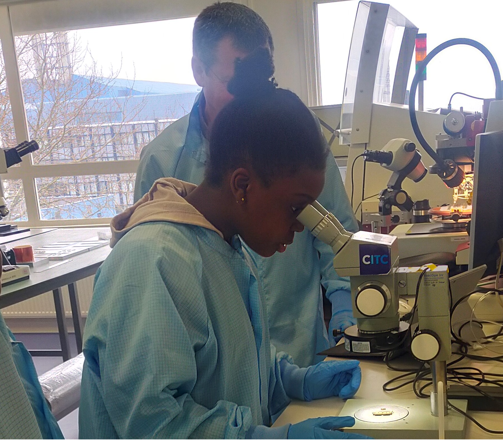
The next part of the program was a lab tour. Before entering the CITC labs, all students were required to dress up in lab coats and gloves. This resulted in a lot of giggles and selfies. Once in the labs, they were able to take a detailed look at equipment such as a die bonder and various microscopes. The students enthusiastically participated: “In the laboratory we were allowed to touch everything. And we could see through a really good microscope. That was cool!”
Practical assignment
The last part of the visit consisted of a practical assignment. The students were to build so-called ‘vibrating robot animals’ (in Dutch: bibberbeestjes). Using tools as screw drivers and cutting pliers, this turned out to be not an easy, but also a very fun task. Again, this lead to a lot of giggles once the batteries were in place and the robot animals vibrated on the tables.
Weekendschool Nijmegen location manager Chris van Wieren noticed how eager his students were. “Looking through a microscope, a machine that does what you say on command, a huge elevator in which machines are transported… you could see the wonder in the students’ eyes during our visit. They are already curious about the world of technology. To further enthuse them, all you need are professionals who can talk passionately about their daily work. Now, thanks to CITC, our students have become a bit more knowledgeable.”
Access to education
Providing access to education is one of CITC’s core activities. By enthusing children at an early age for technology in general, and perhaps a technical education and profession more specifically, we want to contribute to the future of the semiconductor industry in Europe.
Please feel free to contact us if your school is also interested in a CITC guest lecture or company visit.
February 7, 2022 – On February 1, Mudit Goyal, bachelor student in Mechanical and Mechatronics System Engineering, started his internship at renowned provider of advanced packaging solutions Boschman. Keeping in mind that Mudit barely knew anything about the semiconductor industry a year ago, it is clear to see the impact the CITC/HAN Semiconductor University Program has made.
Triggered by webinar
In 2016, Mudit (24), who is originally from India, moved to Germany to realize his dream of working in the automotive industry. He commenced studying Mechanical Engineering at Rhine-Waal University of Applied Sciences, followed by a second bachelor’s degree in Mechatronics. “Last year, the university hosted a webinar about the semiconductor industry,” tells Mudit. “This was very informative and triggered my interest. I remember when COVID-19 broke out, global chip shortages were all over the news. However, it was not until this webinar that I realized that there is a lot of mechanical engineering involved in manufacturing chips.”
One of the speakers during the webinar was Joop Bruines, education consultant at CITC and organizer of the CITC/HAN Semiconductor Packaging University Program. Mudit continues: “Joop also discussed this program and after some research, I decided to subscribe to the minor. It supported both my bachelor courses perfectly.”
Pragmatic approach
The university program kicked off in September 2021. Together with 18 other students, Mudit attended lectures by people working at semiconductor companies such as NXP, Sencio, Enzyre and Nexperia. He was pleased with the input of the industry experts: “I think we covered the entire semiconductor industry from the 1980s-2020s in just 2.5 months. It’s probably still the tip of the iceberg, but I’ve learned so much about the backend industry. I liked the approach of the program the most. It’s very pragmatic: we studied real-life problems rather than theoretical situations you see in textbooks.”
The minor has just finished. “Lately, we were working in groups of four students on our practical assignments. Originally, we were going to do these in the CITC labs. COVID-19 unfortunately prevented this. However, Joop provided a very good and challenging alternative assignment that we could work on. I can really recommend this course to students who want to get to know the semiconductor industry and as such make an informed decision about their future career.”
Boschman internship
As of February 1, Mudit has continued with his bachelor’s thesis project: an internship at Boschman, a high-tech, solution driven Dutch company focusing on advanced packaging solutions. “Joop acted as a broker and recommended me by dropping my resume during a visit. I cannot wait to begin work there and gain more experience in this industry.”
After the internship at Boschman, Mudit hopes to determine whether he will continue his studies and obtain a master’s degree in power electronics. But what about his dream that brought him to Europe in the first place? He smiles: “I have not forgotten that! Nowadays, electrification and automation of car has increased the use of chips for manifolds. So after I graduate, I intend to work I the automotive sector.”
February 2, 2022 – Providing access to education is one of CITC’s core activities. We regard education and training as crucial to secure the future of the semiconductor industry in Europe. In addition to our Semiconductor Packaging University Program, we therefore offer internships and graduation assignments to students. Two of our recent students share their CITC experience.
Marley Hoban – internship
In June 2021, Marley Hoban joined CITC for an eight-month internship project. A Mechanical Engineering student from the University of Limerick in Ireland, Marley (21) is in his third year of his bachelor’s degree.
Nijmegen is not the most obvious location for an internship when you are studying in Ireland. Marley explains how he ended up at CITC: “The university distributes our CVs to all the companies it is affiliated with. In my case, CITC picked me and a few other students to interview. After a few rounds of interviews, I was offered an internship.”
Excellent crossover with university
Marley’s project involved adapting a reflow soldering machine for use as a pressure-assisted sintering machine – an interesting mix of practical and theoretical challenges. He comments: “My internship assignment had excellent crossover with my degree. My assignment consisted of designing and building a machine. In doing so, I used many of the skills I had learned in university, like CAD modelling, materials science, coding and metal machining skills.”
He continues: “Before I began, I was not sure what to expect. I had heard stories from friends that did internships in other companies, and they were given boring, menial tasks. However, after starting work, I was pleasantly surprised at how interesting my work was and how much responsibility I was given.”
Encouraging and helpful colleagues
An internship involves more than just a technical assignment; the development of social and collegial skills is also important. Marley describes his internship as an enjoyable experience. “The CITC team is small, welcoming and a pleasure to work with. All my colleagues were encouraging and helpful towards my project. The overall work environment was really nice.”
When asked to characterize his internship in three words, he chooses stimulating, educational and challenging. “I would definitely recommend CITC to other students. CITC ensures that the student’s project is well suited to the degree. Students are given a lot of freedom to approach the problem as they wish. They also have access to excellent lab facilities and experienced scientists, engineers and businesspeople to consult with.”
Bas Braakhekke – graduation assignment
In September 2021, Bas Braakhekke (22) joined CITC for his graduation assignment. Bas is studying Engineering Physics at Fontys University of Applied Sciences in Eindhoven. He found CITC’s assignment in the university’s weekly newsletter. “The assignment immediately appealed to me”, says Bas. “The underlying theory was interesting and the assignment itself was clearly worked out.”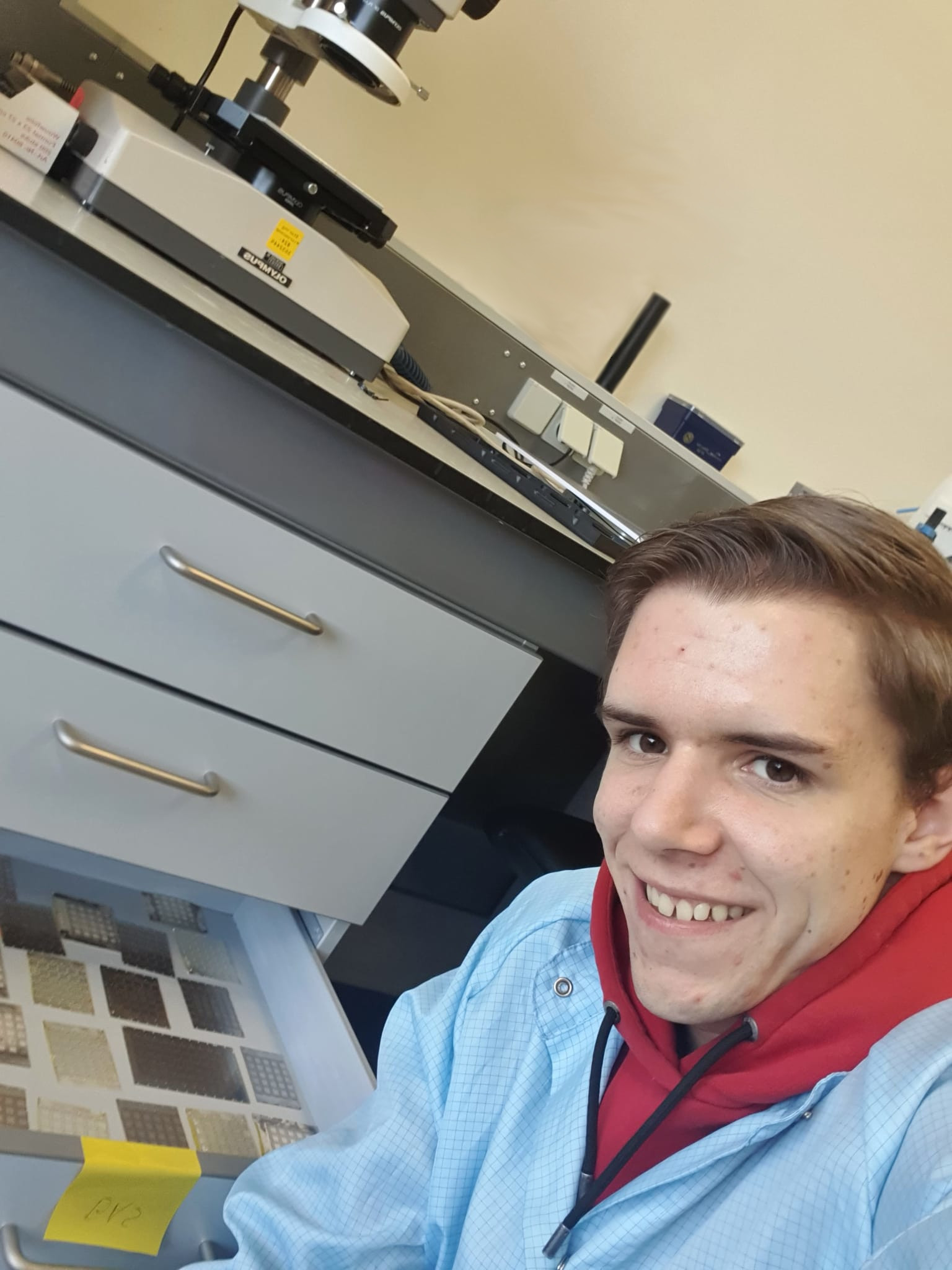
Combination of new and familiar topics
Bas’ assignment consisted of optimizing the settings of CITC’s plasma cleaner. He explains: “The goal was to provide the best possible surface for gold-gold and silver-gold wire bonding. I have examined the effect of the cleaning settings by contact angle analysis, wire pull and shear strength tests.”
Semiconductors were hardly covered during his education, so the industry was unknown territory for Bas. “Many topics and their theoretical background were new to me. However, I was acquainted with the measuring methods and techniques like plasma cleaning and contact angle analysis. I think the project has become a well-balanced combination of new topics and familiar material.”
Great place to work
During Bas’ time at CITC, he was part of a group of five interns. One of them is also a Fontys student from Eindhoven, so they regularly carpooled to Nijmegen. Just like Marley, Bas enjoyed his time at CITC. “I can certainly recommend CITC when you’re looking for an internship – especially if you live close to Nijmegen. The campus is a really nice place to work and if I hear about its plans for the future, it will get even better.”
Bas was happy with his assignment, the supervision and the freedom to operate. “What I liked most, however, were the colleagues at CITC. Because it is a small club, I got to know everyone, either on the work floor or on our team outing. And of course it was very nice to work with many peers.”
When also asked to characterize his internship in three words, Bas picks sociable, hands-on and research. “It’s a great place to work for students!” On January 26, Bas presented and defended his final report – successfully awarded an 8.
Wanted: new students
Interested in an internship or graduation assignment at CITC? Check out the opportunities or send an open application.
PRESS RELEASE | Nijmegen, the Netherlands, January 20, 2022
On January 20, Chip Integration Technology Center (CITC) and AntenneX signed an agreement to formalize their collaboration. Both organizations are active in the RF domain, especially in 100 GHz+. Together, they address the characterization needs for next generation high-frequency packaging applications.
Due to the need for more and more bandwidth in wireless communication, the next generation communication standard (6G) is set to operate at frequencies around and above 100 GHz. From an electronic packaging point of view, this means a widespread adoption of antenna-in-package (AiP) type of devices where the antenna system is integrated into the device package.
This high degree of integration, combined with high operational frequencies, poses several challenges – not only for production, but also for the characterization of materials and performance of the AiPs. At these high frequencies, material characterization and over-the-air device measurement simultaneously become more important and challenging. Therefore, CITC and AntenneX work together to address the characterization needs for these kinds of packaging applications.
Novel packaging technologies and concepts
Francesca Chiappini, Program Manager RF Chip Packaging at CITC, is pleased with the collaboration: “Working with AntenneX is a welcome addition to our current ecosystem. They enable us to develop novel packaging technologies and concepts for higher frequencies. For measurements at lower frequencies, we are already working with the TNO Radar Technology department. With AntenneX, we can now cover the frequency spectrum beyond 100 GHz. They help us tackle issues such as dielectric material characterization and antenna measurements at frequencies of relevance for 6G and automotive radar.”
Complementary services
Sander Bronckers, one of the founders of AntenneX, adds: “Our services are complementary to CITC’s activities. When developing new equipment, tools and software, CITC helps us by providing extensive feedback. And they support us in defining requirements for measurements, analysis and characterization. Last, but not least, CITC has a large network. By working together, we can offer our tools and services to companies better and more easily.”
– ENDS –
About CITC
Chip Integration Technology Center (CITC) is a non-profit joint innovation center specializing in heterogeneous integration and advanced chip packaging technology. CITC has created an effective ecosystem in which companies, research and educational institutes work on bridging the gap between academics and industry. CITC’s contribution to the ecosystem is to provide access to innovation, infrastructure and education.
www.citc.org
About AntenneX
AntenneX offers in-house antenna measurements and material characterization up to 140 GHz for applications such as wireless communications, car radar, 5G/6G, Internet-of-Things, medical imaging, remote sensing, and more. AntenneX supports your design of a wireless device by quantifying and interpreting the over-the-air performance via tools or services.
www.antennex.tech