Master thesis project: Sub-mm printing process evaluation of copper sinter paste for copper pillars on all printed SMD components
Synopsis
There is an industrial interest to lower the costs of current manufacturing processes for printed SMD components. Through printing, resistive elements can be produced but the challenge remains with bumping. Replacing expensive metallization processes with printed copper pillars can potentially reduce product costs, processing steps, and facilitates flip-chip bonding. Copper sintered pillars favor soldering unlike silver which suffers from diffusion of solders.
Challenges
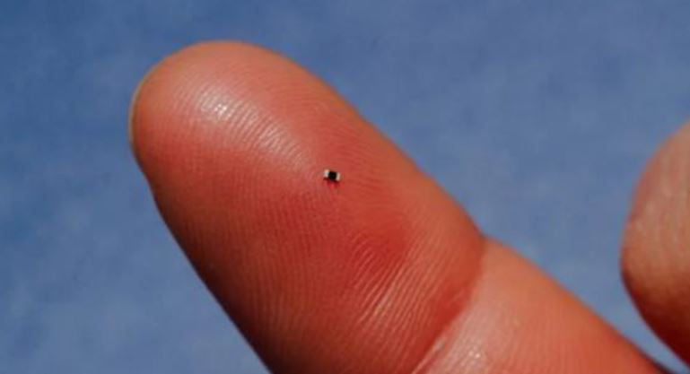
Figure 1a Thin Film resistor in 0402 package [1]
The printable area on such small footprints would be in sub-mm range (tentatively 0.2mm x 0.4mm).
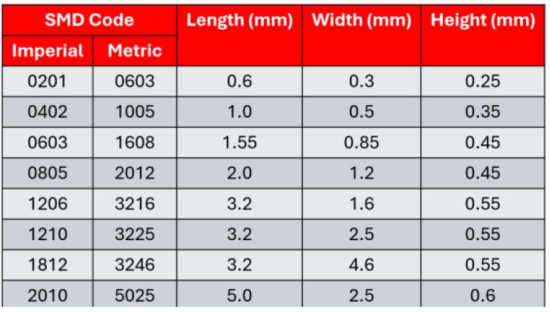
Figure 1b: SMD chip resistor sizes and codes [1]
- Conventional screen printers lack the necessary resolution to reach sub-mm printing
- An aspect ratio of at least 1 is required
- Strong adhesion to the substrate
- A target bump thickness – 20 to 30 𝜇m
Project objective
Investigate different processes for printing different sizes of copper pillars that are compatible with various SMD codes. The expected project flow is as follows:
- Material scouting – exploring potential printable copper pastes and their curing processes (pressure/pressureless)
- Material testing – conduct some preliminary material tests to evaluate the bond strength to Ag
- Printing process analysis – evaluate screen/stencil printing resolution limitation using DEK printer at TNO/CITC and further explore photolithographic stencil printing [2] at TNO Holst Centre
- Prototype printing – demonstrate successful printing over a large substrate with SMD components
- Explore the advantages and drawbacks with comparison to other processes
- Final presentation internally at CITC and Master thesis defense
Note: the process of thesis writing goes hand-in-hand throughout the process flow
Internship and MSc thesis details
- Location: flexible at CITC in Nijmegen and TNO Holst Centre in Eindhoven
- Collaborators: CITC
- Duration: 6 – 8 months
- Requirements: current MSc students in Mechanical or Electrical Engineering
- Supervisors: Henry Antony Martin and Edsger Smits
- Internship stipend: standard internship stipend provided by CITC. Travel allowance can be discussed
Contact us
If you would like to learn more about CITC, this internship assignment or what we can offer you, please contact us.
References
[1] https://www.ultralibrarian.com/2020/06/02/0402-package-footprint-resistor-sizes-and-parameters-ulc
[2] Ji, X., Du, L., He, S., van Zeijl, H.W., & Zhang, G. (2023). Microstructural and micromechanical characterization of sintered nano-copper bump for flip-chip heterogeneous integration. Microelectronics Reliability